Time:2019-12-05 Browse times:706second
|
Equipment name: |
Cutting film |
|
Manufactor: |
DENKA |
|
Model: |
Cutting film |
|
Particular year: |
|
|
Equipment status: |
|
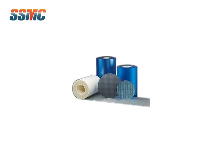
Back Grinding Tape -P Series-
A back grinding tape (hereafter as BG tape) is used for protecting the
circuit surface from scratches, chipping / crack and particle
contamination, during the back-grinding process. The functions of BG
tapes are (1) protecting workpiece surface from contamination, (2)
highly close contact to workpiece and (3) easiness of peeling, and
higher technology to those functions is required with the developments
of jumbo-sized and thinned wafer and high-bumped wafer. Elegrip BG tapes
produced by DENKA do not require to rinse your workpiece after BG
process due to excellent adhesive. We Toyo Adtec consider needs of each
user and choose appropriate tapes.
Feature
Excellent contact to asperity of the circuit side
Effective control of particle
Good water-seepage control
Excellent grinding accuracy (TTV)
Easy peeling
Effective control on adhesive deterioration with time
|
Product Number |
Base Film |
Color |
Total Thickness |
Adhesive Thickness |
|
BGE-122S |
EVA |
LB |
140 |
20 |
|
BGE-122V |
||||
|
BGE-1240A6 |
160 |
40 |
||
|
BGE-124S |
||||
|
BNY-1250A3 |
170 |
50 |
||
|
BNY-1250A4 |
||||
|
BGE-164VC |
200 |
40 |
*The above data is just for representing value, and not guaranteed value.
*Color : MW (Milky White), B (Llight Blue), T (Transparent)
*Separator thickness is not included.
Our company acts as agent for DENKA tape in Japan. The former name of DENKA tape is Toyo tape
DENKA tape includes four films:
1. BG tape, grinding protective film, which is divided into UV type and non UV type.
2. Non UV tape, cutting film, usually blue or white.
3. UV tape, cutting film, can also be used for grinding protection.
4. Peeling tape, used for uncovering after grinding.
Application fields:
1. Grinding protection of semiconductor wafer
2. Cutting process of semiconductor wafer
3. Cutting process of semiconductor back section substrate / copper frame
4. Cutting process of ceramic substrate
5. Cutting process of LED base plate
6. Glass product cutting process
Characteristic:
1. As the agent appointed by DENKA, we have sufficient samples of different types and sizes in our factories in Suzhou and Shenzhen for our customers to choose and test.
2. We have a special UV film application laboratory, which can choose tape according to the actual products of customers, provide cutting test, and finally evaluate whether our products are suitable for the application of customers.
3. Our company is engaged in grinding and cutting OEM business. We have safety stock for common membranes. We can provide emergency delivery support for our customers.